Tag: hardware

external memory board


Just before writing my last post, I started building another board in order to supply my ATmega128 with 64Kbytes of external memory (in fact the so called “XMEM” feature was one of the reasons I bought that chip).

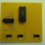
The board is designed for a 28 pin S-RAM IC (Hitachi HM6264) that can be connected to a micro controller supporting external memory (like the ATmega128 or ATmega162) using three 10 pin headers. The first header is used for the multiplexed lower address/IO bits (port A on micro controller), the second for dedicated upper address bits (port C) and the last for read/write strobe and address latch enable (port G). All headers share two common last pins: GND (9) and VCC (10). The only thing required except for the S-RAM itself, some pin headers and a 100uF ceramic capacitor is a octal latch IC (74AHC573) that will allow for multiplexing the shared lower address/IO lines.

NOTE

After looking up the “Address Latch Requirements” section in the ATmega128 datasheet turns out that when the micro controller is operated above 8MHz (mine has a 16MHz crystal) the 74HC573 (the IC I have) does not meet requirements but a 74AHC573 would do. I guess I will put in a 8MHz crystal until I can get hold of a 74AHC573.


Download
base board for Olimex ATmega128 header board


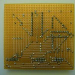
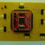
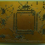
A couple of months ago I ordered a ATmega128 header board (AVR-H128) from Olimex. In order to make use of such a header board you need to mount it somewhere. For this purpose I created a sort of header board for the header board. It is very minimal, consisting of mechanical components only except for a LED and a resistor. The reason for that is that the header board on which the ATmega128 itself is placed already contains a +5V voltage regulator (LM78L05) and reset circuit (ZM33064). Using my board its very convenient connecting things to the pins of the micro controller. All ports (A, B, C, D, E, F and G) have a separate 10 (2×5) pin header where the last two pins of each header is connected to GND (9) and VCC (10).

The layout of the board was created with the intention in mind to be able to assemble it in a through-hole fashion. Needless to say that the layout can also be used to etch or mill the board.

There are still things that can be enhanced like adding a connector for the reference voltage of the ADC (AREF).

Download

Schematics and layout have been created using Eagle 5.11 with a non-commercial license. The outline of the board is 100x160mm, so for you folks that use the Eagle freeware you will not be able to modify the boards layout (since Eagle as freeware only allows for boards with a outline of 100x80mm).