Tag: photo

lzoDSO – finished prototype board assembly

Posted by May 14, 2013

P1070973_modified_medium-1024x768_modified

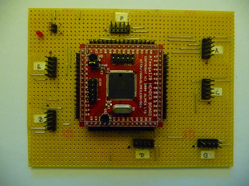
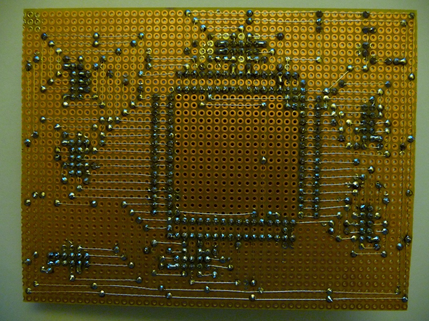
Yesterday I finished the assembly of the new front panel controller board, which evolved out of the old display carrier board). The circuit signal lines have  already been tested (using continuity testing) and I’m not far away from having the prototype be contained inside its case.

In the new board I basically merged the core board with the display carrier board, since there was enough space available. A slight change I introduced is that I adjusted some pin mappings (namely we moved the LCD control lines from port B to D).

Schematic and Circuit Board

PDF files for schematic and board.

schematic board

Now I’m updating the wiki page of the prototypes to get things in sync again.

lzoDSO – hardware prototype

Posted by April 11, 2013

IMG_0257_modified-small
lzoDSO hardware prototype

Recently I have been working on my oscilloscope project. Documenting ideas, digging out requirements and restructuring the whole projects documentation wiki. While doing so I realized that the page was totally confusing to new visitors since it does not say that there is no finished scope yet (even though there is a picture of one). What one can see on the pictures is actually a prototype. Until now we did not explicitly say so. This is NOT the final thing.

To address that issue we added a Status section to the start page of the wiki that clarifies the projects state.

Now the interesting part: We created a new page for the prototype which is linked on the wikis start page and moved existing files related to the components of the prototype from /trunk to /branches/prototype-a.

Next step will be to take the legacy firmware we have and adjusted it to make it run on the prototype hardware. When the firmware is ported (basically adjust pin mappings, enable/disable functionality) we will use is as the starting point to get the code incrementally refactored until we replaced everything with test-driven code.

external memory board


Just before writing my last post, I started building another board in order to supply my ATmega128 with 64Kbytes of external memory (in fact the so called “XMEM” feature was one of the reasons I bought that chip).

The board is designed for a 28 pin S-RAM IC (Hitachi HM6264) that can be connected to a micro controller supporting external memory (like the ATmega128 or ATmega162) using three 10 pin headers. The first header is used for the multiplexed lower address/IO bits (port A on micro controller), the second for dedicated upper address bits (port C) and the last for read/write strobe and address latch enable (port G). All headers share two common last pins: GND (9) and VCC (10). The only thing required except for the S-RAM itself, some pin headers and a 100uF ceramic capacitor is a octal latch IC (74AHC573) that will allow for multiplexing the shared lower address/IO lines.

NOTE

After looking up the “Address Latch Requirements” section in the ATmega128 datasheet turns out that when the micro controller is operated above 8MHz (mine has a 16MHz crystal) the 74HC573 (the IC I have) does not meet requirements but a 74AHC573 would do. I guess I will put in a 8MHz crystal until I can get hold of a 74AHC573.


Download

base board for Olimex ATmega128 header board


A couple of months ago I ordered a ATmega128 header board (AVR-H128) from Olimex. In order to make use of such a header board you need to mount it somewhere. For this purpose I created a sort of header board for the header board. It is very minimal, consisting of mechanical components only except for a LED and a resistor. The reason for that is that the header board on which the ATmega128 itself is placed already contains a +5V voltage regulator (LM78L05) and reset circuit (ZM33064). Using my board its very convenient connecting things to the pins of the micro controller. All ports (A, B, C, D, E, F and G) have a separate 10 (2×5) pin header where the last two pins of each header is connected to GND (9) and VCC (10).

The layout of the board was created with the intention in mind to be able to assemble it in a through-hole fashion. Needless to say that the layout can also be used to etch or mill the board.

There are still things that can be enhanced like adding a connector for the reference voltage of the ADC (AREF).

Download

Schematics and layout have been created using Eagle 5.11 with a non-commercial license. The outline of the board is 100x160mm, so for you folks that use the Eagle freeware you will not be able to modify the boards layout (since Eagle as freeware only allows for boards with a outline of 100x80mm).